Northbridge (computing)
Jump to navigationJump to search
|
This article needs additional citations for verification. (January 2008) (Learn how and when to remove this template message)
|
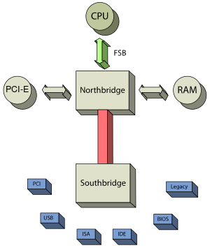
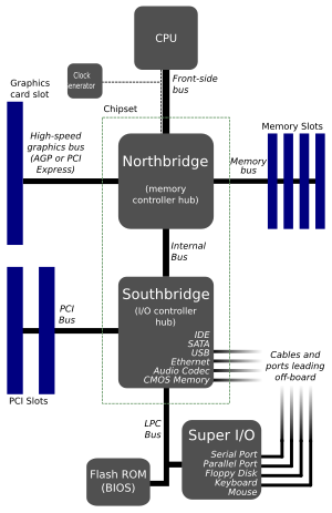
A northbridge or host bridge is one of the two chips in the core logic chipset architecture on a PC motherboard, the other being the southbridge. Unlike the southbridge, northbridge is connected directly to the CPU via the front-side bus (FSB) and is thus responsible for tasks that require the highest performance. The northbridge, also known as Memory Controller Hub, is usually paired with a southbridge.[1] In systems where they are included, these two chips manage communications between the CPU and other parts of the motherboard, and constitute the core logic chipset of the PC motherboard.[2]
On older Intel based PCs, the northbridge was also named external memory controller hub (MCH) or graphics and memory controller hub (GMCH) if equipped with integrated graphics. Increasingly these functions became integrated into the CPU chip itself,[3] beginning with memory and graphics controllers. For Intel Sandy Bridge and AMD Accelerated Processing Unit processors introduced in 2011, all of the functions of the northbridge reside on the CPU,[4] while AMD FX CPUs still require external northbridge and southbridge chips.
Separating the different functions into the CPU, northbridge, and southbridge chips was due to the difficulty of integrating all components onto a single chip.[5] In some instances, the northbridge and southbridge functions have been combined onto one die when design complexity and fabrication processes permitted it; for example, the Nvidia GeForce 320M in the 2010 MacBook Air is a northbridge/southbridge/GPU combo chip.[6]
As CPU speeds increased over time, a bottleneck eventually emerged between the processor and the motherboard, due to limitations caused by data transmission between the CPU and its support chipset.[7] Accordingly, starting with the AMD Athlon64 series CPUs (based on the Opteron), a new architecture was used where some functions of the north- and southbridge chips were moved to the CPU. Modern Intel Core processors have the northbridge integrated on the CPU die, where it is known as the uncore or system agent.
Overview[edit]
The northbridge typically handles communications among the CPU, in some cases RAM, and PCI Express (or AGP) video cards, and the southbridge.[8][9] Some northbridges also contain integrated video controllers, also known as a Graphics and Memory Controller Hub (GMCH) in Intel systems. Because different processors and RAM require different signaling, a given northbridge will typically work with only one or two classes of CPUs and generally only one type of RAM.
There are a few chipsets that support two types of RAM (generally these are available when there is a shift to a new standard). For example, the northbridge from the Nvidia nForce2 chipset will only work with Socket A processors combined with DDR SDRAM; the Intel i875 chipset will only work with systems using Pentium 4 processors or Celeron processors that have a clock speed greater than 1.3 GHz and utilize DDR SDRAM, and the Intel i915g chipset only works with the Intel Pentium 4 and the Celeron, but it can use DDR or DDR2 memory.
Etymology[edit]
The name is derived from drawing the architecture in the fashion of a map. The CPU would be at the top of the map comparable to due north on most general purpose geographical maps. The CPU would be connected to the chipset via a fast bridge (the northbridge) located north of other system devices as drawn. The northbridge would then be connected to the rest of the chipset via a slow bridge (the southbridge) located south of other system devices as drawn.

Intel i815EP northbridge
Overclocking[edit]
The northbridge plays an important part in how far a computer can be overclocked, as its frequency is commonly used as a baseline for the CPU to establish its own operating frequency. This chip typically gets hotter as processor speed becomes faster, requiring more cooling. There is a limit to CPU overclocking, as digital circuits are limited by physical factors such as rise, fall, delay and storage times of the transistors, current gain bandwidth product, parasitic capacitance, and propagation delay, which increases with (among other factors) operating temperature; consequently most overclocking applications have software-imposed limits on the multiplier and external clock setting. Additionally, heat is a major limiting factor, as higher voltages are needed to properly activate field effect transistors inside CPUs and this higher voltage produces larger amounts of heat, requiring greater thermal solutions on the die.
Evolution[edit]
The overall trend in processor design has been to integrate more functions onto fewer components, which decreases overall motherboard cost and improves performance. The memory controller, which handles communication between the CPU and RAM, was moved onto the processor die by AMD beginning with their AMD64 processors and by Intel with their Nehalem processors. One of the advantages of having the memory controller integrated on the CPU die is to reduce latency from the CPU to memory.
Another example of this kind of change is Nvidia‘s nForce3 for AMD64 systems. It combines all of the features of a normal southbridge with an Accelerated Graphics Port (AGP) port and connects directly to the CPU. On nForce4 boards it was marketed as a media communications processor (MCP).
AMD Accelerated Processing Unit processors feature full integration of northbridge functions onto the CPU chip, along with processor cores, memory controller and graphics processing unit (GPU). This was an evolution of the AMD64, since the memory controller was integrated on the CPU die in the AMD64.
The northbridge was replaced by the system agent introduced by the Sandy Bridge microarchitecture in 2011, which essentially handles all previous Northbridge functions.[10] Intel’s Sandy Bridge processors feature full integration of northbridge functions onto the CPU chip, along with processor cores, memory controller and graphics processing unit (GPU). This was a further evolution of the Westmere architecture, which also featured a CPU and GPU in the same package.[11]


